
T-ray vision
An international team of researchers has developed an innovative method to observe what happens inside electronic chips while they are in operation, without needing to turn them off, disassemble them, or even touch them.
The new technique is based on the already well-known terahertz waves, or T-rays, a safe and non-ionizing form of electromagnetic radiation that is being extensively researched for use in innovative medical examinations, as it produces images without the risks of other techniques.
The THz band is a vast and still largely unexplored frequency range because only now are technologies capable of operating with it beginning to be developed. It’s like Superman’s “X-ray vision” without the risks of X-rays.
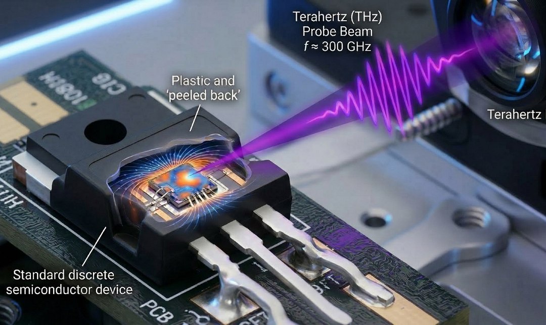
Now, for the first time, terahertz radiation has been used to detect minute movements of electrical charges within fully encapsulated semiconductor devices, allowing monitoring of what happens inside electronic components operating in the real world.
Once a chip is sealed inside its protective packaging, it is extremely difficult to know what is happening inside, limiting diagnostics, troubleshooting, or monitoring of how specific chips function under varying environmental conditions.
“Most existing inspection methods require physical electrical probes, exposed chips, or switched-off devices, making them impractical in many scenarios,” commented Professor Withawat Withayachumnankul of the University of Adelaide, Australia. “This research is a first step towards solving a long-standing problem in electronics. We can now observe the electrical activity inside a functioning semiconductor device from the outside without damaging it or interrupting its operation.”
[Image: Bryce Chung et al. – 10.1109/JMW.2026.3653411]
Monitoring of functioning chips
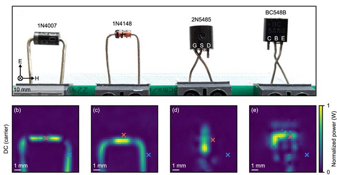
In principle, terahertz waves should indeed be able to probe encapsulated and active semiconductor components by detecting changes in electron density passing through the junctions that form transistors. But, in practice, it is not at all simple to probe a millimeter area at a frequency in the 275 GHz range and accurately pinpoint the area of a PN junction, which is much smaller than the wavelength.
The team solved this by creating a new type of detector, a homodyne quadrature receiver, which proved capable of canceling background noise and isolating the weak signal produced by the electrical activity of electronic components.
“Due to the high sensitivity of this transceiver, subwavelength targets can be effectively monitored with conventional terahertz optics. These experimental results demonstrate the ability of terahertz waves to non-invasively monitor the activity of semiconductor devices,” the team wrote.
This demonstration paves the way for non-destructive inspection of chips during production and for monitoring devices in operation.
“Being able to remotely and non-invasively assess electronic activity can help verify the integrity of critical hardware, detect faulty or compromised components, and monitor systems where physical access is limited or undesirable,” said Chitchanok Chuengsatiansup of the University of Potsdam in Germany. “This research paves the way for smarter, self-diagnostic electronics, new ways to monitor complex integrated circuits, and faster development of next-generation chips.”
Source: www.inovacaotecnologica.com.br
Source link