
It has been almost four decades since the first demonstration of the ability to move individual atoms, which led scientists to consider the possibility of building objects from the bottom up, designing and assembling materials atom by atom, to customize their properties or create materials with characteristics not found in nature.
Progress has been slow. It is true that several techniques already exist that allow the movement of individual atoms, but they only allow the movement of atoms in two dimensions, along the surface of materials. Furthermore, these are extremely slow processes that only work under conditions of high vacuum and cryogenic temperatures.
But the dream continues. Julian Klein and a team from several research institutions have just developed a way to precisely move tens of thousands of individual atoms within a material in minutes, and to do so at room temperature.
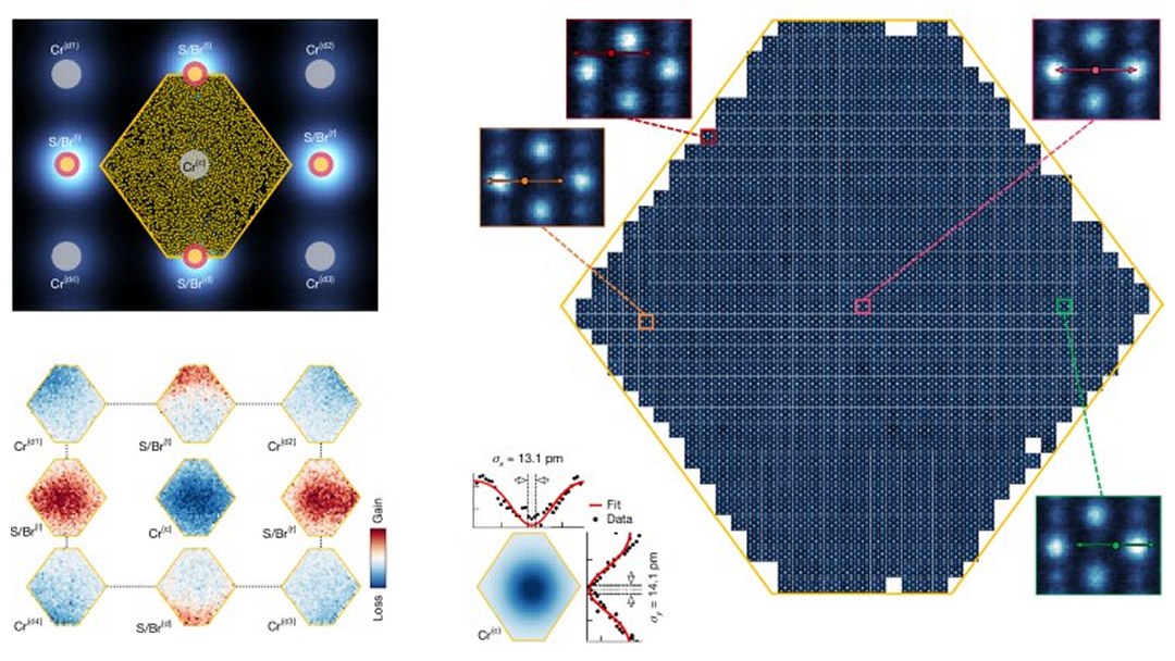
The approach uses a set of algorithms to carefully position an electron beam at specific locations in the material and then sweep the beam to drive the movement of the atoms.
“The results demonstrate the ability to move atoms deterministically and repeatedly within the 3D atomic lattice of a material,” said Klein of MIT. “We can reprogram materials to create defects at will, realizing entirely artificial states of matter not found in nature, with a wide range of potential applications, including sensing, optical, and magnetic technologies. There are countless opportunities made possible by these techniques.”
[Image: Julian Klein et al. – 10.1038/s41586-026-10431-9]
Moving atoms wholesale
It was in 1989 that IBM researchers used a scanning tunneling microscope to arrange 35 atoms on the surface of a crystal cooled to near absolute zero, using the atoms to form the word “IBM”. After that, two other techniques were developed to manipulate atoms in a vacuum, using optical tweezers to trap neutral atoms and oscillating electric fields to trap ions.
Now, for the first time, these manipulations can be performed in three dimensions, reaching the interior of materials. To achieve this, researchers have created algorithms to automatically control some of the world’s most powerful microscopes at Oak Ridge National Laboratory in the USA.
The set of algorithms directs an electron beam to a target atom with an accuracy of a few picometers (one trillionth of a meter). The beam describes a closed loop to help focus on the target, and then sends another electron beam through the material in a carefully designed oscillatory trajectory, remaining for about one second at each point.
“We developed algorithms that allow us to quickly obtain information about the beam’s location in the material,” Klein explained. “The secret is to use very few electrons in the process of obtaining this information, so that the whole process is fast and doesn’t accidentally damage the crystal. It took us many years to develop these algorithms and determine the minimum amount of information needed to infer the location of the atoms with the highest precision.”
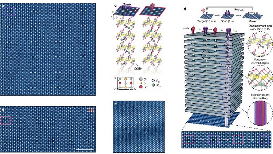
The movement of the beam that supplies the electrons follows an oscillating path, pushing entire columns of atoms to new locations, much like when you slide your finger across your phone screen.
[Image: Julian Klein et al. – 10.1038/s41586-026-10431-9]
Creating engineered material
To demonstrate the technique, the researchers directed the movement of columns of chromium atoms in a stable semiconductor material, chromium sulfide bromide (CrSBr), using a crystal about 13 nanometers thick. The beam created atom-sized vacancies in the material, each vacancy paired with the displaced atom, giving the crystal exotic quantum properties – these new properties still need to be studied.
To demonstrate the scalability of the approach, the team created over 40,000 defects in about 40 minutes, generating vacancies and interstices at different distances and patterns, calculating that different atomic arrangements should result in different quantum mechanical properties.
“Each of these defects has certain ways of interacting with its neighbors,” explained Professor Frances Ross. “If you arrange them into a pattern, you can essentially simulate the interactions between electrons within a molecule, so that the entire electronic structure of that molecule can, in a sense, be mapped onto a pattern that you can etch onto a solid material.”
The researchers claim that their technique lays the foundation for a new class of programmable matter , aiding in the development of a range of quantum devices.
“This is a way to access physical phenomena involving many atoms arranged in a specific array, something that can’t be done by self-assembly,” Ross said. “You can create individually tuned atomic arrangements, and you can have many of them, each arranged exactly as you want in areas of tens and hundreds of nanometers. This leads to a collective physics that we are eager to explore.”
Source: www.inovacaotecnologica.com.br
Source link