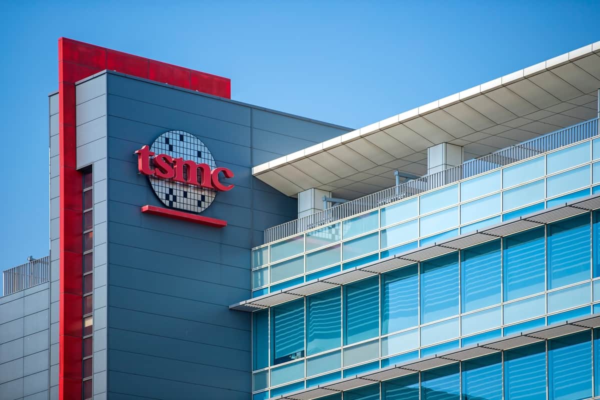
The TSMC the main chip manufacturer for companies like Apple, Nvidia and Google, presented this Wednesday (22) its new generation of production technologies. The big highlight was the statement that the company will be able to deliver smaller and faster components without the need to purchase ASML’s new and very expensive machines, which cost around US$400 million each.
During the North America Technology Symposium in Santa Clara, California, the company revealed two key advances:
- A13: technology aimed at producing very high-performance artificial intelligence chips, expected to start in 2029.
- N2U: a more affordable option designed for both smartphone and laptop processors and AI applications.
Strategy against high cost
TSMC’s decision to optimize its current extreme ultraviolet (EUV) lithography machines rather than move to the new generation “High NA” from Dutch supplier ASML is purely economic. The new machines cost twice as much as previous versions.
Kevin Zhang, senior vice president of TSMC, told Reuters that the company’s Research and Development department has been successful in leveraging existing EUV technology while maintaining an aggressive technical evolution schedule.
The “new” Moore’s Law
While some industry leaders, such as Jensen Huang (CEO of Nvidia), claim that Moore’s Law – which predicts the doubling of computing power every two years – has come to an end, TSMC is trying to keep it alive through a chip “sewing” technique.
Instead of just focusing on reducing the size of a single component, the company is betting on packaging several smaller chips in a single package. According to Dan Hutcheson of TechInsights, Moore’s Law is transforming from a single chip to multiple integrated chips, which allows for continuous gains in power and performance.
Thermal and structural challenges
By 2028, TSMC hopes to be able to combine up to 10 large processing chips and 20 memory stacks into a single assembly. However, this technique brings significant physical obstacles:
- Heat: the simultaneous operation of so many cores generates high temperatures.
- Physical integrity: Different materials expand at different rates under heat, which can cause packages to crack or deform.
According to analysts consulted by Reutersthese problems have already been noticed in Nvidia’s Vera Rubin AI processor. Although TSMC has shown its technological roadmap, experts point out that the company has not yet detailed how it intends to solve these structural engineering challenges in the coming years.
Source: www.olhardigital.com.br
Source link